
Table of Contents
As electronic devices become more powerful, compact, and feature-rich, manufacturers must use advanced component packaging technologies to meet increasing performance demands. One of the most widely adopted packaging solutions in modern electronics is BGA in PCB, which stands for Ball Grid Array in Printed Circuit Boards. This technology has revolutionized PCB design and assembly by enabling higher pin counts, improved electrical performance, and better thermal management compared to traditional component packages.
Today, BGA components are commonly found in smartphones, computers, networking equipment, automotive electronics, medical devices, and industrial systems. Understanding BGA in PCB is essential for engineers, designers, and manufacturers who want to develop reliable and high-performance electronic products.
What Is BGA in PCB?
BGA in PCB refers to the use of Ball Grid Array packages mounted onto printed circuit boards. A Ball Grid Array is a type of surface-mount package that uses an array of small solder balls located underneath the component instead of traditional leads extending from the sides.
These solder balls serve as electrical and mechanical connections between the integrated circuit and the PCB. During assembly, the solder balls are aligned with corresponding pads on the circuit board and permanently attached through a controlled reflow soldering process.

The unique design of BGA packages allows manufacturers to place a large number of electrical connections within a relatively small footprint, making them ideal for high-density electronic applications.
Why BGA in PCB Is Important
Modern electronic devices require increasingly complex integrated circuits with hundreds or even thousands of input and output connections. Traditional package types often struggle to accommodate such high connection densities while maintaining acceptable electrical performance.
BGA in PCB addresses these challenges by offering:
- Higher pin density
- Reduced package size
- Improved electrical performance
- Better thermal dissipation
- Enhanced reliability
- Support for miniaturized designs
These advantages have made BGA technology a preferred choice for advanced electronic products across numerous industries.
How BGA Packages Work
Unlike conventional packages that use leads around the perimeter, BGA packages distribute solder balls across the entire bottom surface of the component.
Each solder ball corresponds to a specific electrical connection. When the component is placed onto the PCB, the solder balls align with matching pads on the board.
During reflow soldering, controlled heating melts the solder balls, creating permanent electrical connections and securing the component to the PCB.
This arrangement allows more connections to fit within a smaller package while shortening electrical signal paths.
Shorter signal paths improve performance by reducing electrical resistance, inductance, and signal distortion.
Types of BGA Packages Used in PCB Assembly
Several variations of Ball Grid Array packages are commonly used in electronics manufacturing.
Plastic Ball Grid Array
Plastic Ball Grid Array packages are among the most widely used BGA types. They provide a cost-effective solution for many commercial electronic applications.
Ceramic Ball Grid Array
Ceramic Ball Grid Array packages offer superior thermal and mechanical performance. They are often used in aerospace, defense, and high-reliability applications.
Fine-Pitch Ball Grid Array
Fine-pitch BGA packages feature smaller solder ball spacing, allowing greater connection density within a compact footprint.
These packages are commonly used in mobile devices and advanced computing systems.
Micro Ball Grid Array
Micro BGA packages are designed for highly miniaturized products where space is extremely limited.
They provide high functionality while supporting compact device designs.
Advantages of BGA in PCB Design
The widespread adoption of BGA in PCB manufacturing is driven by several significant benefits.
High Connection Density
One of the primary advantages of BGA technology is its ability to accommodate a large number of connections within a relatively small package.
This capability supports the increasing complexity of modern integrated circuits.
Improved Electrical Performance
The shorter electrical pathways provided by BGA packages reduce signal delays and improve high-speed performance.
This is especially important in applications involving high-frequency signals and fast data transmission.
Better Thermal Management
Many BGA packages offer improved heat dissipation compared to traditional package types.
Effective thermal performance helps maintain component reliability and supports higher operating speeds.
Compact Product Design
Because BGA packages use the entire underside of the component for connections, they occupy less board space than many alternative package types.
This enables manufacturers to develop smaller and lighter electronic devices.
Enhanced Mechanical Reliability
Properly assembled BGA components can provide strong mechanical connections capable of withstanding vibration and thermal cycling.
Challenges Associated with BGA in PCB
Although BGA technology offers many advantages, it also presents unique manufacturing challenges.
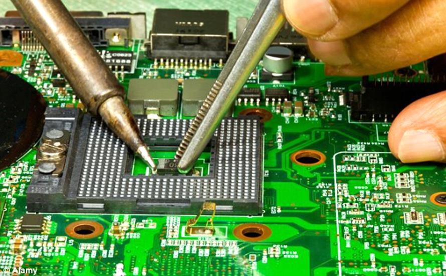
One of the biggest challenges is inspection. Because solder joints are hidden beneath the component body, visual inspection is not possible after assembly.
Manufacturers often rely on X-ray inspection systems to evaluate solder joint quality and identify defects.
Repair and rework can also be more difficult than with traditional leaded packages. Specialized equipment and skilled technicians are typically required to remove and replace BGA components.
Additionally, PCB design considerations such as pad layout, routing strategies, and thermal management become increasingly important when working with BGA packages.
PCB Design Considerations for BGA Components
Successful implementation of BGA in PCB designs requires careful planning.
Engineers must consider factors such as:
- Pad design
- Solder mask configuration
- Via placement
- Signal routing
- Thermal management
- Power distribution
High-density BGA packages often require advanced PCB technologies such as High-Density Interconnect (HDI) designs and microvias to accommodate complex routing requirements.
Proper design practices help improve manufacturability and long-term reliability.
Assembly Process for BGA in PCB
The assembly of BGA components follows a highly controlled manufacturing process.
First, solder paste is applied to the PCB pads using precision stencils.
Automated pick-and-place machines then position the BGA component onto the board with extreme accuracy.
The assembly passes through a reflow oven where carefully controlled temperatures melt the solder balls and create permanent electrical connections.
After soldering, X-ray inspection is typically performed to verify solder joint integrity and identify potential defects such as bridging, voids, or insufficient solder connections.
This process ensures reliable assembly quality and product performance.
Applications of BGA in PCB
BGA technology is widely used across numerous industries due to its ability to support high-performance electronic systems.
Common applications include:
- Smartphones and tablets
- Desktop and laptop computers
- Servers and data centers
- Networking equipment
- Automotive electronics
- Medical devices
- Industrial automation systems
- Aerospace and defense electronics
- Telecommunications infrastructure
Many advanced processors, memory devices, graphics chips, and communication modules utilize BGA packaging.
Future Trends in BGA Technology
As electronic products continue to evolve, BGA technology is advancing to support higher performance and greater integration.
Emerging trends include:
- Smaller package sizes
- Higher pin counts
- Improved thermal solutions
- Advanced substrate materials
- Enhanced manufacturing automation
- High-speed communication support
The growth of artificial intelligence, 5G communications, autonomous vehicles, and edge computing is expected to drive continued demand for advanced BGA solutions.
Manufacturers are also investing in improved inspection technologies and process controls to enhance assembly quality and reliability.
Conclusion
BGA in PCB has become a cornerstone of modern electronics manufacturing, enabling compact designs, high connection density, superior electrical performance, and improved thermal management. By replacing traditional leaded packages with solder ball arrays, BGA technology supports the increasing complexity of today’s electronic devices across industries such as computing, telecommunications, automotive, medical, and industrial automation. While BGA components present unique design, assembly, and inspection challenges, their advantages far outweigh these complexities when implemented correctly. Partnering with an experienced BGA Assembly Service helps ensure accurate component placement, reliable solder joint formation, advanced inspection capabilities, and long-term product performance in demanding electronic applications.